TAN: Trailer Area Network

Introduction

A friend of mine, Scott Lemon founder and CTO of Wovyn, and I were discussing my travel trailer API and he coined the term, trailer area network or TAN. My TAN is going to be based on WiFi because of the ubiquitous availability of WiFi connected devices including microcontrollers, commercially available connected devices, and mobile phones and tablets. To this network I’ll attach microcontrollers that control trailer subsystems. These subsystems will connect via WiFi to a trailer hub that will expose subsystem functionality through the travel trailer API, see Figure below.

In this figure Internet connectivity is acquired through a mobile hotspot with the help of a cell signal booster. The mobile hotspot allows 15 devices to connect to it. One of the 15 devices will be the TAN Hub. The TAN Hub will create a subnet that subsystems will attach to, there could be many. Communications between the subsystems and the TAN Hub may use various protocols, but the TAN Hub will expose their functionality through a REST based API.

Components

There are three main sets of components that are needed to create the described TAN. For Internet connectivity we need a signal booster and a mobile hotspot. We need a server of sorts to act as the TAN Hub and a WiFi connected microcontroller unit to use in the construction of subsystems.

Internet Connectivity

I have selected the AT&T Unite Explore, also known as the Netgear AC815S, device as my mobile hotspot device. It seems to get good reviews and is reasonably priced. I may experiment with other hotspots in the future.

I acquired a weBoot Drive 4G-M Cell Phone Signal Booster to facilitate the acquisition of cell signals in remote locations. In the future I may experiment with various antenna configurations to increase the usable range.

Trailer Area Network Hub

For the TAN Hub I will use the Corewind WiFiG25 microcontroller module described in my original post describing my trailer API. This module is based on a 400 MHz ARM processor, has ample memory, and built in WiFi and runs the Linux operating system.

I expect to add an API management system to this module and communication systems to enable it to connect to and communicate with trailer subsystems.

Subsystem Controllers

There are many potential trailer subsystems that can be exposed and interacted with through an API. Examples include: leveling jacks, stabilizers, tank levels, battery levels, solar energy generation, awning, pop-outs, security, weather data, etc. Each of these will inevitably require special sensors, actuators, etc., but I am hoping to standardize on the microcontroller modules used to control the subsystems and communicate to the TAN Hub.

I will be experimenting with the ESP 12-F module based on the ESP8266 chip. This is an impressive module featuring a 32 bit MCU, integrated WiFi, tcp/ip stack, 4 MBytes of Flash memory for user programs, and all this for $1.74. It is capable of communicating with other hardware using SPI, I2C, Serial and other low level communication protocols.

These communication channels, as well as the available GPIO lines, will be used to interface these modules to subsystem specialty hardware such as switches, sensors, etc. The integrated WiFi will be used to connect these subsystems to the TAN Hub.

Summary

Future posts will describe various details related to the programming, configuration, and use of the components discussed in this post. There is much to learn, much to do, and a lot of fun to be had.

Travel Trailer API

Introduction

I have recently purchased a travel trailer and desire to instrument and automate it. I want to control and monitor all of its systems using my iPhone or other mobile devices. When I am out in the sticks (defined by my son to be wherever there is no Internet connectivity) I want to connect to the trailer’s systems via a local WiFi network. When the trailer is in a location where LTE, or other data services are available, I want to interact with the trailer via the Internet.

While there are many systems to monitor and control, there are two fundamental technological pieces they all require. First, a WiFi network must be provided for mobile phones and other devices to connect. Second, a central controller is needed to manage the myriad of systems that will be connected to this network and manage the associated API.

Rather than boiling the ocean, I intend on focusing on one simple representative system, a weather station, and connecting it to our trailer. Success with this system requires solving many issues that will simplify the inclusion of additional systems in the future. The rest of this post will describe a path forward. A series of future posts will describe the details associated with each subsystem.

System Description

The goal of this project is to enable a mobile phone user to view weather data acquired from a weather station connected to our travel trailer. There are a number of modules or subsystems required to accomplish this:

  1. A mobile phone that connects to a WiFi network and an application that consumes an API that returns weather station data.
  2. A secure WiFi network or trailer area network (TAN). While security of weather station data may not be required, future projects will require it and we should design with security in mind.
  3. A central controller that connects to the provided TAN and exposes an API management tool. This will enable mobile phones and other devices to access available data in a secure and managed way.
  4. A 433 MHz receiver connected to a microcontroller based module will convert the signal acquired from the weather station into an appropriate API.
  5. A weather station that transmits collected data on the 433 MHz band.

The weather station will collect environmental data and transmit it over the 433 MHz radio frequency band. This signal will be acquired using a 433 MHz receiver that converts this analog signal to digital for consumption by a microcontroller based system. The digital signal will be parsed appropriately and exposed through an API. This API will be managed by the central API management system and exposed to other devices over trailer area network. The mobile phone will consume this API and an appropriate mobile phone app will present it to the user.

Chosen Components

There are many possible components to choose from to accomplish the goal and steps outlined above. The components I’ve chosen and describe below are simply representative of the myriad of possible choices.

Weather Station

I will use the AcuRite 5 in 1 Professional Weather Center model 01536. This product is compact, easily mounted on a trailer and broadcasts weather data on the 433 MHz band. The outdoor component measures the temperature, humidity, rainfall, wind speed and wind direction. This data is combined into a packet and broadcast periodically. The indoor component is a nice color display that displays this data and archives previously received data. The indoor and outdoor components are paired through a simple channel selection mechanism.

433 MHz Receiver

I acquired the Sunkee 433 MHz superheterodyne wireless receiver module to convert the analog signal broadcast from the weather station into a digital signal appropriate for consumption by a microcontroller based system. This module can operate from roughly 3 to 5 Volts and requires a simple wire antenna. It outputs a digital signal easily read by standard microcontrollers.

Microcontroller System

I have chosen to use the Corewind WiFiG25 microcontroller module. It has a 400 MHz ARM processor, plenty of memory, built in WiFi connectivity, numerous I/O lines of various types, runs the Linux operating system, supports many programming languages, and only costs about $30.

Software Components

With the receiver connected to the microcontroller module, the rest is up to the software. A simple program will be written to acquire the digital I/O data from the receiver and store it in memory. The Kong API management tool will be implemented on the microcontroller to expose the collected weather data via an API. This API can then be consumed over the WiFi network by a mobile phone and associated application and our task will be complete, for now.

Summary

The components described above, and a few others, will be combined to expose weather data via an API for consumption by mobile phones and potentially other devices. The next post will describe the setup and use of the receiver module and a description of the data collected from the weather station. A series of posts will follow describing the remaining steps to accomplishing our goal.

myDoorbell: Play that Tune

Introduction

In a previous post, I described the nine modules that make up myDoorbell. These are shown in the following figure. In this post I’ll address two modules that are difficult to describe separately, the microcontroller near the center of the figure and the MP3 decoder to its right.

Basic Operation

In my previous post I described a circuit that will translate a doorbell button press to a signal appropriate for consumption by the microcontroller. When this signal is received by the microcontroller, it takes two actions:

  • It raises a signal to the second microcontroller enabling it to raise external events. These events will be discussed in a future post.
  • It reads a MP3 encoded audio file from the memory and writes it to the MP3 Decoder module.

The MP3 Decoder module receives the streamed data from the microcontroller and decodes it, resulting in a small signal audio output.

The Microcontroller and Software

The microcontroller chosen for this application is the Atmel Atmega 328P. This processor is simple to use, relatively inexpensive and more than meets the requirements for this portion of myDoorbell. The schematic below illustrates the circuit used for this application. The labelled input and output signals are grouped into several main functions:

  • Input from the doorbell button detection circuit described in the previous post.
    • FBELL_BUTTON and RBELL_BUTTON
  • Output signals to the second microcontroller.
    • FBELL_EVENT and RBELL_EVENT
  • Serial Peripheral Interface (SPI) signals for communicating to the MP3 decoder and programming this microcontroller
    • BELL_SCK, BELL_MISO and BELL_MOSI
  • Memory control and data signals
    • MEM_SEL, MEM_GRANT, MEM_REQ, MEM_RESET, MEM_RDY and MEM_SB
  • MP3 decoder control and data signals
    • VS_XCS, VS_XDCS, VS_DREQ, VS_RESET and MUTE
  • An external clock running at approximately 8 MHz.
    • EXT_CLK 

The LED and the associated current limiting resistor are available as a programmable output that is easily visible. This can be used to indicate state or for initial debugging. The push button enables the device to be manually reset. The capacitors are 0.1 µF devices that act as bypass capacitors, see Basics to Remember below. The six pin header, in the upper right corner of the schematic, is for programming the microcontroller.

The software that drives the signals identified above can be found in the myDoorbell repository on github.com. While there is considerable amount of detail, that is best addressed by viewing the source code, a brief overview is useful.

The “main” routine initializes the memory module and the MP3 Decoder module by communicating with them over the identified control and data lines. This communication takes place using the SPI protocol. This routine then loops checking the state of the front and rear doorbell buttons and requesting or relinquishing control of the memory device to / from the second microcontroller.

If the front or rear doorbell buttons are pressed, the microcontroller accesses its built in EEPROM to determine the volume at which the ringtone should be played. It then plays the appropriate ringtone for the front or rear door.

The ringtone is played by determining its length and repeatedly reading portions of it from the memory and streaming it to the MP3 decoder. When the data is consumed the device goes back to checking the state of the doorbell buttons.

The MP3 Decoder

The MP3 decoder is based on the VS1011 MP3 Audio Decoder. The following schematic is recreated from it datasheet.

The input and output signals, on the left of the schematic, are connected to the identically named signals from the microcontroller schematic already presented. The outputs on the right are the two audio output signals and the common between them. Lots of bypass capacitors and a few other components, as illustrated in the datasheet, are included.

The VS1011 is capable of consuming MP3 and WAV formatted audio files and generating low level audio output. The audio output is sufficient to drive a pair of headphones, but in our application will drive an audio amplifier and associated speaker.

A Failed First Attempt 

The first design had a serious flaw that only manifested itself when in use. This misstep led to the design described in this post. However, since this design was put into use, two others have been proposed and will be described later.

The first design had a single microcontroller that interacted with the WiFi module, the doorbell button circuitry, the memory and the MP3 decoder. There was a major issue with this approach. When the doorbell button was pressed, should the MP3 file be played before an event is sent to the user, such as a text message, or should the event be raised and then the ringtone played?

If the event is sent first it will delay the playing of the ringtone by at least hundreds of milliseconds, but often much more. This doesn’t sound like much, but when you push a doorbell button you expect to hear the bell. In practice it was very odd to push the button and not get immediate feedback.

If you play the ringtone first and then send an event it works great, unless someone picks a 30 second ringtone. In this case, by the time you receive the text message and arrive at the door, the person is long gone. I have personally found that this behavior is often a feature, but others disagree.

This issue led to the design described here where we have two processors that communicate via shared signals and a shared memory. This approach is obviously more complex and more expensive.

Physical Implementation

The schematic for the microcontroller shown above resulted in the following PCB layout.

This design required a few traces to be routed on the bottom layer. As with previous PCBs illustrated in this series of posts, this one also utilizes a 4-layer design with internal layers carrying ground and 3.3 V. The reset button is on the far left, the microcontroller in the center and its programming header on the right.

The schematic for the MP3 decoder, illustrated above, results in the following 4-layer PCB. The crystal that controls the clock for this unit is located on the left of the layout. Most of the input and output lines are located at the bottom of the board. The low level

audio output interface is located on the right. As in previous layouts, bypass capacitors and other components are placed as close to the device as possible. 

Two Alternative Designs

The first alternative design is based on the initial single CPU misstep. In the first design the problem was dealing with which came first, the raising of external events or the playing of the ringtone. A better approach may be to send the MP3 decoder the first 32 bytes of MP3 data and then start raising the external event. The MP3 decoder has a data request (DREQ) line that gets asserted whenever the decoder is capable of receiving another 32 bytes of MP3 data. If this were tied to the microcontrollers interrupt line it could be used to direct the microcontroller to send more audio data and then return to raising the event. The only question is whether the 8 MHz microcontroller is fast enough to switch between the two tasks and accomplish what needs to be done without introducing gaps in the ringtone.

Back of the envelope analysis to figure out if this would work goes something like this. Good quality stereo MP3 files are about 1 Mbyte per minute in size. Since we only need one channel we can reduce the file size to 500 Kbytes per minute. We can clock SPI data into the MP3 module at 4 MHz or 4 Mbits per second. With 8 bits per byte this translates to 500 Kbytes per second. With switching time between tasks and other overhead this won’t work, but it is likely that we can get by with far less quality than we expect from our digital stereo music. Reducing the quality will likely make this technique possible.

The second alternative design takes a radically different approach. For this approach we trade out the WiFi module, both microcontrollers, memory, and the MP3 decoder and replace it with a fast embedded ARM microcontroller that runs the Linux operating system. An example of this is the Onion, shown below.

The microcontroller runs at 400 MHz instead of 8 MHz, giving us plenty of horsepower to accomplish our task. The Linux operating system provides the task switching necessary to switch rapidly between raising external events and playing ringtones. Audio playback software can be used instead of the dedicated MP3 decoder hardware currently being used. Finally, this sort of board costs less than $20, which is less than the WiFi module used in the current approach. This approach is currently being pursued.

In my own defense let me state that these sorts of modules were not available when the first design was completed. In addition, education leads to doing things in a better way; I’ve learned a lot!

Outcomes and Artifacts

There are likely many ways to build this portion of myDoorbell and a few of them have been described. The Eagle schematic and PCB files are available from the myDoorbell repository at github.com.

Basics to Remember

Bypass capacitors are used in many digital systems. Each clock cycle a digital system has the potential to change from one state to another. When this occurs the device draws significantly more current for a very short period of time. Recall that every wire acts like an inductor and that inductors resist changes in current. If the PCB trace from the device to the power source is long or narrow it will restrict current sufficiently to starve the device from the energy that it needs during these transition periods. Bypass capacitors hold sufficient charge to supply the device with the needed energy during these short periods of time. They are recharged while the device is relatively stable. These capacitors should be located as close to the device as possible and located between the power source and the device. This close proximity will reduce the inductance of the connecting trace.

myDoorbell: The Button

Introduction

In my previous post, I described myDoorbell’s power supply module. In this post I will describe the circuitry that translates a standard doorbell button press into something that can be easily consumed by a microcontroller.

Standard Operation

The standard doorbell circuit is shown in the following figure. Recall that when the doorbell button is not pressed (open), current flows from the transformer, through the lamp, and through the solenoid, completing the circuit. With the doorbell button open, my test setup has approximately 50 mA of current. When the button is pressed (closed) a larger current, approximately 1 A, flows through the circuit.

myDoorbell is complicated by the system requirement to use the existing doorbell button and retain the functionality of its lamp.

myDoorbell Button

The figure above can be represented by a schematic where the lamp is replaced by a 320 Ω resistor. We model the lamp with this value resistor because with 16 Vrms across it,  the current flow is ~50 mA.

myDoorbell does not need the solenoid in the above circuit. However, if we simply replace it with a wire we will create a short circuit when the button is closed. In this case, approximately 0 Ω will exist, resulting in nearly infinite current, a bad idea. So replacing the solenoid with a resistor, to limit current, is necessary, but what value still needs to be determined. A large value resistor will result in little current, which is attractive, but too little current and the lamp won’t be bright enough to be useful.

As previously discussed, resistors have resistance values measured in Ω’s, but they are also rated for the amount of power they can dissipate. The power dissipated by a resistor is equal to the product of the voltage across it and the current through it. Through manipulation of Ohms Law it can be shown that the power dissipated by a resistor is also equal to the product of its value and the square of the current through it. With this in mind, if we choose a low value resistor its power rating will need to  be increased.

For example, if we choose a 10 Ω resistor, for the top resistor in the above figure, then approximately 48 mA will flow through the lamp when the button is open. The 10 Ω resistor will have to dissipate 0.02 W, well below the 0.1 W rating typical for small surface mount resistors. However, when the button is closed 1.6 A will flow through the circuit and the resistor must dissipate 25.6 W, it’s going to catch fire!

Let’s choose a higher value resistor, say 10 kΩ. Now when the button is open approximately 1.6 mA of current flows through the circuit resulting in the 10 kΩ resistor dissipating just 0.02 W, which is great, but the lamp will be very dark, bad!

So let’s compromise. We’ll choose a 220 Ω resistor that results in a current flow of 29 mA and a lamp that is visible when the button is open. In this mode the 220 Ω resistor will dissipate 0.185 W. This will require a larger resistor, but manageable. When the button is closed the 220 Ω resistor results in a current of nearly 73 mA and a power dissipation of 1.17 W. This will require quite a large surface mount resistor, but is necessary to meet our design requirements.

Detecting the Press

When the button is open, the voltage across it is equal to 320 Ω * Ilamp. Where Ilamp is equal to 16 Vrms / 540 Ω, or 29 mA. So the voltage across the button when it is open is 9.48 Vrms. When the button is closed, the voltage across it is 0 V. What we need is a circuit that detects this difference and generates a DC voltage appropriate for an input to a 3.3 V microcontroller. The figure below depicts just such a circuit. 

To the left we see the portion of the circuit described earlier, consisting of the transformer, push button, the 320 Ω resistor representing the lamp, and the 220 Ω resistor added to restrict the current flow when the button is closed. The circuitry to the right needs explaining.

Let’s start with the component outlined in the rectangle, an optocoupler. This device consists of a LED that emits infrared light onto a light sensitive driver. When the input current is sufficiently high, infrared light is emitted by the LED, and the output of the driver is pulled to ground. When the input current is sufficiently low, the output is left in an “open collector” state where no current flows. With no current through the output resistor, there is no voltage drop across it. In this state, the output level is equal to the voltage attached to the other side of the output resistor, in our case 3.3 V. A representative device is the H11L1M. Its datasheet can be found here.

In our application, when the doorbell button is closed there is 0 V across the LED of the optocoupler and the output will be 3.3 V. When the button is open the 320 Ω resistor, representing the lamp, will have 9.48 Vrms across it. The peak voltages are -13.4 V and 13.4 V. According to the optocoupler’s datasheet, its LED cannot tolerate reverse voltages exceeding 6 V, so the external diode is added to protect it. The external diode conducts when the input voltage is negative, resulting in roughly 1 V across the LED. 

Again referring to the datasheet, we need 1.6 mA of forward current on the LED to get the device to activate, driving the output low. As the input voltage rises from 0 V to 9 V we’ll allow the output to remain high, but when it arrives at 9 V we’ll switch the output to low. This will result in a 60 Hz sequence of 3.3 V pulses while the button is open. To accomplish this we need the optocoupler input current to be less than 1.6 mA with input voltages less than 9 V, and greater than 1.6 mA when the input voltage are higher.

Imagine we don’t know the value of the 5600 Ω resistor in the above circuit. To meet the requirements described in the previous paragraph, we need to size this resistor appropriately. If there is 9 V on the left of the resistor and 1 V on the right side, due to the forward voltage drop VF across the LED, there is 8 V across the resistor. This is explained by Kirchhoff’s Voltage Law that states that the sum of voltages around a loop must be zero. To get 1.6 mA at 8 V we need a 5 kΩ resistor, we’ll use the more common 5600 Ω device. At our peak voltage of 13.4 V, we’ll have 2.2 mA of current through the optocoupler’s LED, well below the 30 mA maximum value the device can handle. 

If the optocoupler’s output signal is tied to the input line of a microcontroller, a simple software missing pulse detector can be used to detect when the doorbell button is closed, see the sample below. In this example we check the value of the optocoupler’s output once each ms for one 60 Hz cycle, or one 17 ms period. If it is ever zero the button is open.

Physical Implementation

The complete schematic, with component values, power ratings, and tolerances, is shown below. Component tolerance describes the range of possible actual values of a component as a percentage of their ideal value. If our 5600 Ω resistor has a 10% tolerance, then a real device may have a resistance value as low as 5040 and as high as 6160, with the actual value being somewhere between these extremes. It is important to take these minimum and maximum values into consideration during a design.

Our design is sensitive to the value of R3, the 5600 Ω resistor. For this reason we chose a device with a 1% tolerance. This costs a bit more, but in this case it was important. Also note that we chose a 3W resistor for R1 to ensure we don’t have a catastrophic failure, a fire!

The printed circuit board layout for the above design is shown below. The pads on the far left are for TB1 which is a connector where the two wires from the doorbell button are connected. Notice R2 in the lower right hand corner of the PCB. It is the 680 Ω output resistor and is a normal sized surface mount resistor. Compare this to the size of R1 which is the 220 Ω 3 W resistor, quite large in comparison.

This circuit results in a simple layout that doesn’t require a 4-layer PCB. However, to simplify connections to other myDoorbell modules, a 4-layer technology was used. No routing on the bottom of the board was required. The inner layers are used for ground and 3.3 V and are brought to the top layer using the three visible vias.

When integrated into the final system, small changes were made to optimize the overall layout. In the above photo of the myDoorbell button detection module, you’ll notice that the two smaller resistors and the diode have been move to slightly different locations. The final system contains two of these modules, one for the front door and the other for the rear door.

Outcomes and Artifacts

This post describes a simple circuit and associated software that meets the requirements of keeping the doorbell lamp functional and detecting when the button is pressed. There are likely many alternative techniques for meeting these requirements, but one worth considering is to use an AC line monitor chip such as the MID400 which is intended to raise a signal if the power line voltage is interrupted. In our scenario it would raise a signal if the AC voltage across the doorbell button was absent, or in other words, the button is pressed. This unit costs slightly more than the circuit described above, but would eliminate the need for the external diode and the missing pulse detector software. The output could be tied to a microcontroller interrupt line making the system more responsive, reliable, and perhaps simpler.

The Eagle schematic and PCB files are available from the myDoorbell repository at github.com.

Basics to Remember

The power dissipated by a resistor is equal to the product of the voltage across it and the current through it, P = VI. However, we often don’t know the voltage across a resistor, but rather know the resistance value and the current through it. In this case a simple manipulation of Ohm’s Law yields a solution, P = I2R.

The sum of voltages around a circuit loop must be zero. This fact is known as Kirchhoff’s Voltage Law. It is useful for circuit analysis and as used in this post to determine the proper circuit element values to meet requirements.

myDoorbell: The Power Supply

Introduction

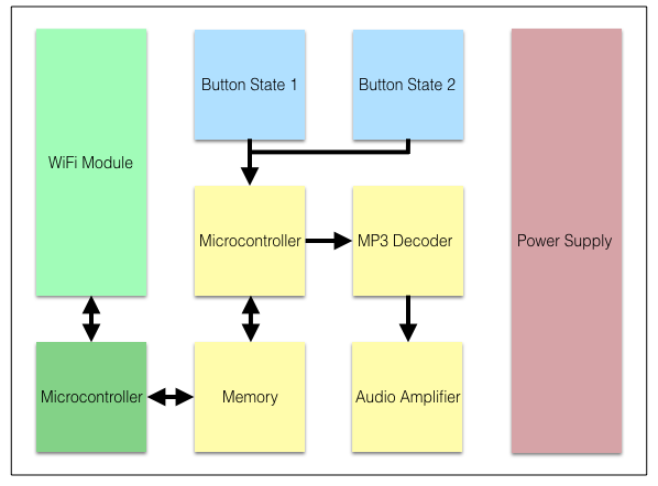
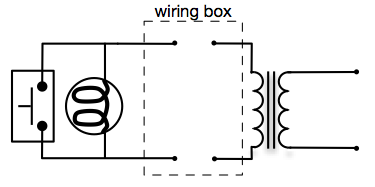
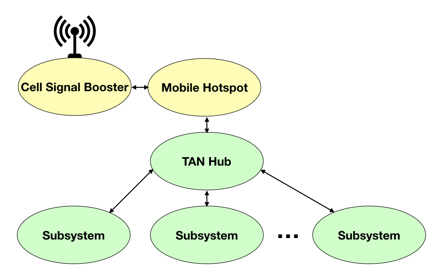
In my previous post, I described the nine modules that make up myDoorbell. While we could begin our discussion with any one of the nine modules, the one all others are dependent on is the power supply. What the power supply is intended to do is convert the source characteristics we have, to the supply characteristics we need. In other words, it needs to convert the 16 volt (V) alternating current (AC) available in the doorbell-wiring box to a direct current (DC) voltage appropriate for our use.

What myDoorbell Needs

Reviewing the datasheets of components, likely to fulfill the function of each of the other eight modules, led me to believe that seven of the eight modules need a 3.3 volt (V) supply. The Audio Amplifier module is the exception.

Audio amplifiers are designed to take small signal inputs and accurately reproduce them with additional power. Like the other modules, the amplifier is powered by a DC source. Since power is equal to the product of voltage and current, it is possible to increase the power of the output signal by increasing its voltage, current or both. It is impractical to use the 3.3 V DC source for the audio amplifier given that we have an upper bound on the available current of just over 1 ampere (A). This combination would result in a 3.3 watt (W) (3.3 V * 1 A) maximum output power. This is insufficient power to drive a speaker at the volume necessary for a doorbell. The better option is to convert the 16 V AC source to the highest voltage DC source conveniently available.

So myDoorbell needs are simple, a 3.3 V DC supply for the digital components and the highest practical DC voltage available for the Audio Amplifier module.

Basic DC Power Supply

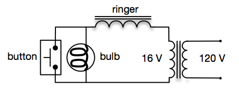
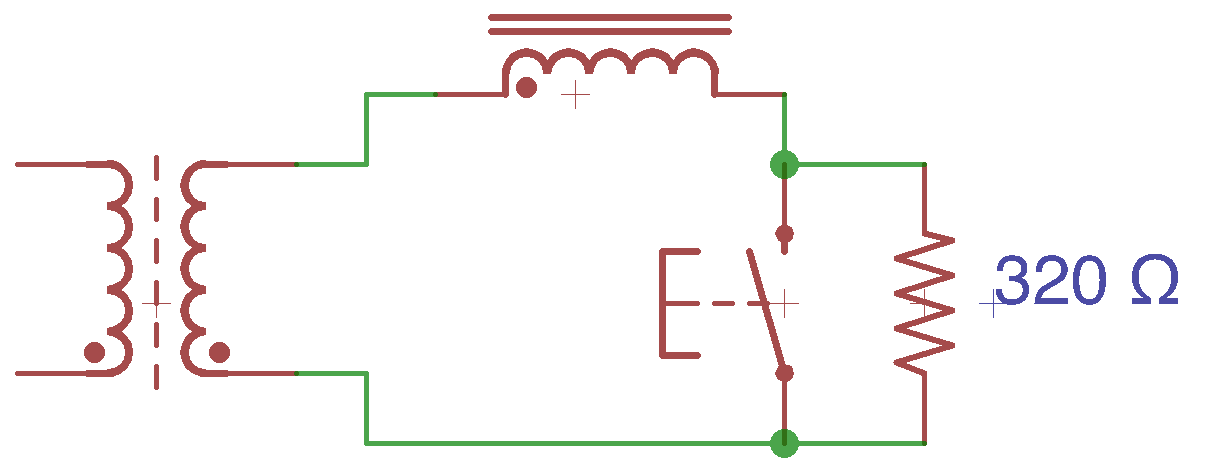
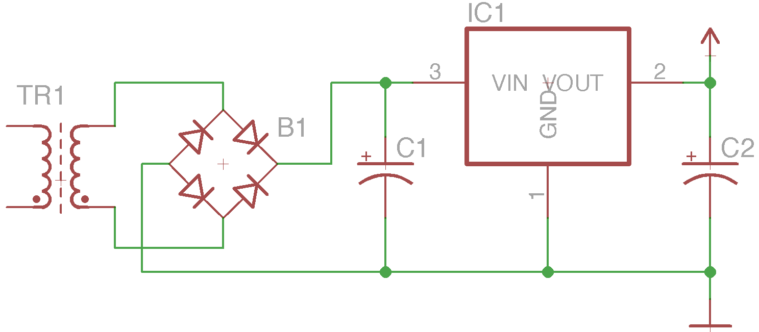
A simple DC power supply is illustrated below. The AC input is connected to the primary terminals on the left of  transformer, TR1. This AC input is a sine wave that swings from a negative to a positive peak with a frequency in the U.S. of 60 cycles per second, or 60 Hz. AC voltages are typically described in terms of their root-mean-squared or rms values. Their peak and rms values are related by, Vrms = 0.707 * Vpeak. In the U.S. a common input voltage is 120 Vrms.

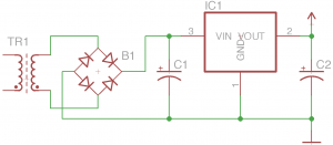
In a typical application, the transformers job is to reduce the input voltage to a voltage just slightly above the desired power supply output voltage. For example, if the desired output voltage is 3.3 V DC, a transformer that transforms 120 Vrms to 5 Vrms may be appropriate. A typical transformer works by having two electrically insulated coils of wire wrapped around a common ferrite core. The coil connected to the input is called the primary, while the other is called the secondary. The ratio of turns on the secondary to primary coils determines how the secondary voltage compares to the primary voltage. For the above example, the primary coil should have 120 V / 5 V = 24 times as many turns as the secondary.

The full-wave bridge rectifier, B1, inverts the negative half-cycles of the transformers output voltage and passes both half-cycles to the output of the rectifier. While this output is DC, the waveform has significant ripple, varying from zero to the positive peak at 120 Hz. The ripple is reduced by capacitor C1 which brings the voltage across C1 to nearly the peak value of the rectifiers output. IC1 is an integrated linear voltage regulator that typically takes a voltage input higher than the desired output voltage and locks its output to the target voltage. Finally, C2 reduces the remaining ripple to tolerable levels.

Continuing with our example, the output of the transformer is 5 Vrms. The full-wave bridge rectifier creates a 120 Hz DC voltage that varies from 0 V to 5 V / 0.707 or 7.07 V. Capacitor C1 reduces the ripple and presents a fairly constant 7.07 V DC input to the voltage regulator. The voltage regulator locks its output to the desired 3.3 V level and most of the remaining ripple is removed by capacitor, C2.

myDoorbell Power Supply

It took me three attempts to find a satisfactory design for the myDoorbell power supply. Recall that the goal is a DC power supply that can power seven of the eight modules at 3.3 V DC and the amplifier with the highest voltage conveniently available. The seven digital modules consume a total of approximately 300 mA or 0.3 A of current at 3.3 V. To provide a margin of safety we will design the power supply to provide 500 mA. The DC voltage at the input of the voltage regulator is equal to 16 Vrms / 0.707 or 22.6 V DC. This will be used for the Audio Amplifier module.

Attempt 1 – Linear Voltage Regulators

The most straightforward DC power supply design for myDoorbell follows the design pattern illustrated earlier. In this simple design the voltage regulator is a simple three pin linear regulator. However, through sad experience this approach doesn’t work in this application because of the large difference between the 22.6 V regulator input voltage and the desired 3.3 V DC power supply output. In our earlier example, the designer was free to pick a transformer that reduced the input supply voltage to a reasonable level. In the myDoorbell world we are stuck with the doorbell transformer that reduces the 120 Vrms line voltage to the available 16 Vrms. This results in the 22.6 V regulator input voltage and the issues using the linear regulator.

The power dissipated by the linear voltage regulator is equal to the product of the voltage across the device and the current through it.

Pregulator = Vregulator * Iregulator
Pregulator = (Vin – Vout) * Iregulator
Pregulator = (22.6 V – 3.3 V) * 0.5 A
Pregulator = 19.3 V * 0.5 A
Pregulator = 9.6 W

This is a significant amount of power that is presented as heat. Without a significant metal heatsink being thermally attached to the voltage regulator it will consume itself. In fact my first design did just that. I was taught that digital electronic systems work because of magic smoke contained in them. When I naively built and tested this design the device overheated, the magic smoke escaped, and the device no longer functioned. While this power supply design is not feasible for myDoorbell, it might effectively test your smoke detectors.

Attempt 2 – DC to DC Converter

After licking my wounds of defeat I came across a device that I thought would fit my needs perfectly, a DC to DC converter. This device is essentially a small power supply integrated into a single package. This device accepted a broad range of input voltages and output 3.3 V at up to 500 mA, a perfect fit.

However, the particular device I chose had a “feature” that caught my eye as a positive thing, but ended up being a show stopper. The grounds on the input and output of the chosen device were isolated. This sounds like a good thing, but after prototyping myDoorbell and debugging for a significant amount of time, a serious design flaw was discovered.

Recall that the audio amplifier will operate from the highest DC voltage conveniently available to us. Well the highest voltage available is the DC voltage just before the DC to DC converter. The voltage available at that location is 22.6 V and is ideal for our audio amplifier. However, the digital electronics will be operating on the opposite side of the DC to DC converter. This includes the MP3 to audio converter that outputs the low voltage audio signal to be amplified. Voltage is an across variable or the potential across two points, typically the signal and a reference ground. In this particular design the MP3 decoder and the audio amplifier share the signal line, but not a common reference. If these grounds are connected, the DC to DC converter does not function properly, if they are not connected, the audio subsystem does not work. Another failure!

After making another design choice, I discovered that there are DC to DC converters that are non-isolated. While this would have worked, a better design in terms of cost exists.

Attempt 3 – Switching Voltage Regulators

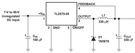
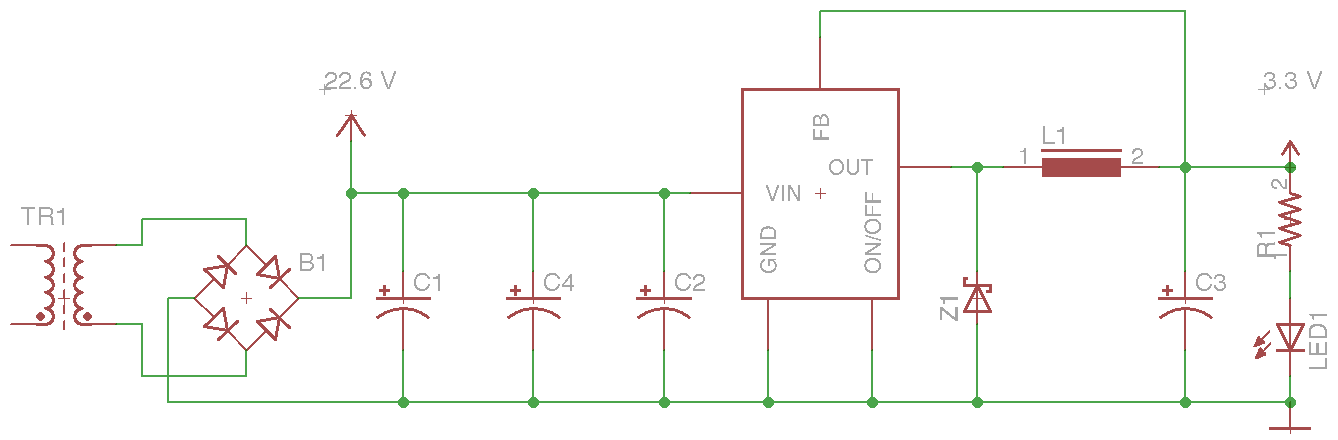
Switching voltage regulators are an alternative to the linear device discussed above. A very simplistic description of how this device operates goes something like this. The device checks the voltage across the capacitor on its output and if it is below the target voltage, the device charges the capacitor. If the voltage on the capacitor is at or slightly above the desired voltage, the device allows the capacitor to discharge. This switching occurs thousands of time per second resulting in small swings between minimum and maximum values. This regulator dissipates far less power and can easily function without a heatsink. The tradeoff is that this device requires a few more components as shown in the following figure taken from the Texas Instruments TL2575 datasheet.

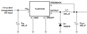
According to the datasheet capacitor Cin stabilizes the regulator, Cout reduces ripple on the output, while diode, D1, and inductor (coil), L1, reduce high frequency noise. The design, shown below, comes from the datasheet with some slight modifications. According to the datasheet, the size of the inductor depends on the output voltage and current characteristics. Referring to the graph included in the datasheet, we chose a 0.001 Henry, 1 mH, inductor. My complete and successful design is illustrated below. 

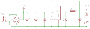
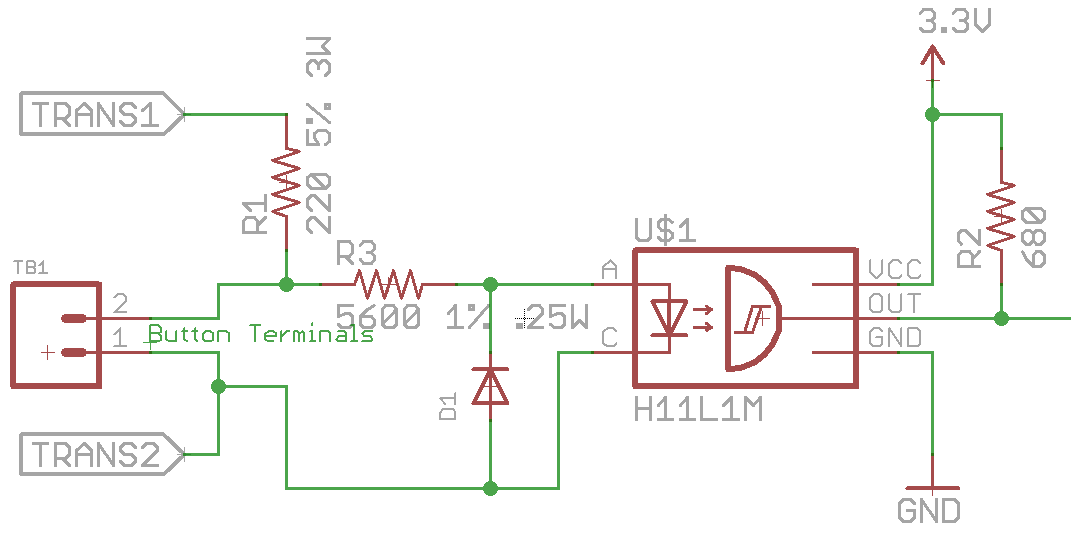
The light emitting diode (LED) and resistor R1 were added to yield a simple power on indicator. The transformer, TR1, is the doorbell transformer and is shown solely for clarity and is not included in the final design. The voltage available after the full-wave bridge rectifier is approximately 22.6 V of smoothed (filtered) DC, perfect for our audio amplifier. The final output is our desired 3.3 V regulated and smooth DC supply, perfect for the remaining digital components making up the system.

Physical Implementation

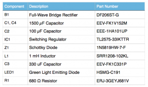
This section describes the design process used to implement the above schematic in a surface mount printed circuit board (PCB). We begin by identifying the components that are required, see below.

While I used the Eagle computer aided design (CAD) tool to input the above schematic and realize the PCB output files, any reasonable tool will do. Most PCB tools have thousands of predefined library components, but I prefer to build my own library parts because I suffer from the dreaded, not invented here syndrome.

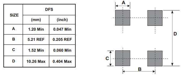
I will illustrate my process for building these library components for the full-wave bridge rectifier, but the same process would be followed for all components used. From the rectifier datasheet we can extract the “suggested pad layout”. If the datasheet for a particular device does not include this, then I select another vendor’s product, that simple! The pad layout is the copper pattern that will be left on the PCB where this device is electrically and mechanically connected using solder. The suggested pad layout for the full-wave bridge rectifier, DF206ST-G, is shown below.

This pattern is added to the library of components and associated with the components schematic drawing. This process is completed for all necessary components.

The schematic is built by placing the selected components and wiring them as illustrated. In Eagle you then convert this to a PCB that results in each component being placed on the PCB with lines connecting the appropriate signal pins. The components are moved into appropriate positions by the designer and the lines are replaced with copper interconnects either automatically or by hand.

Printed circuit boards are made up of layers of conductive material, such as copper, separated by layers of insulation. Layers can be connected through a via. The top and bottom layers are typically covered with a material that doesn’t easily adhere to solder. These layers have openings where solder and components are to be connected to the copper traces.

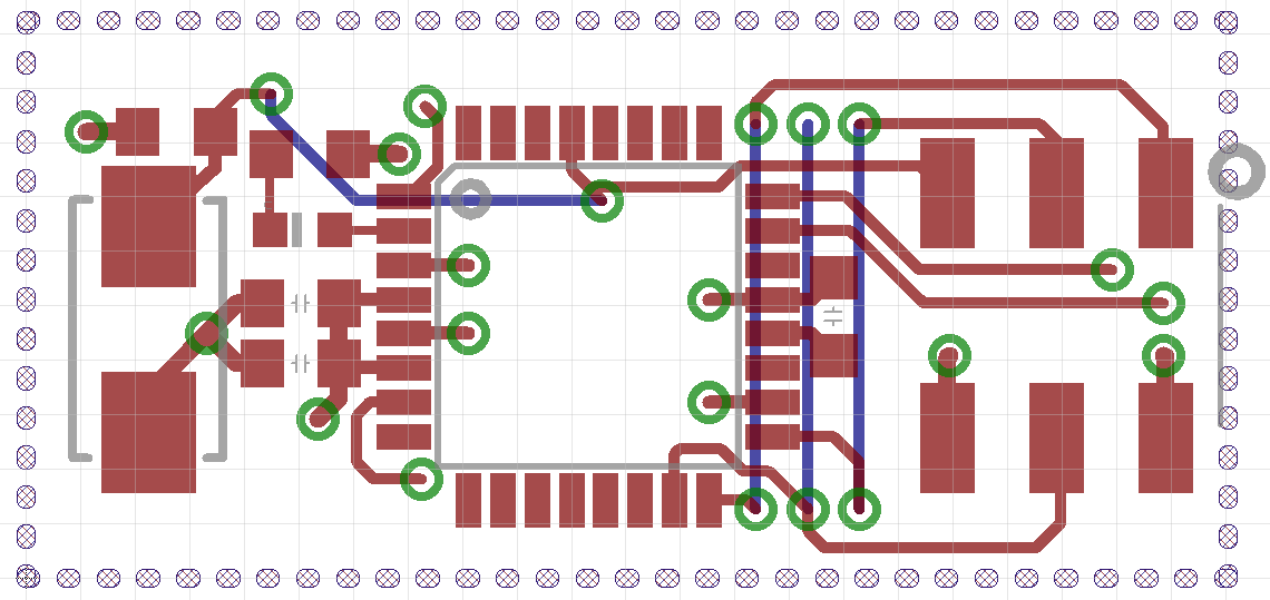
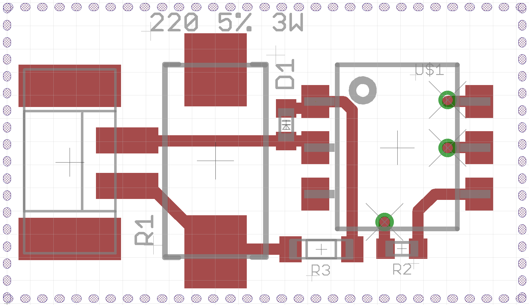
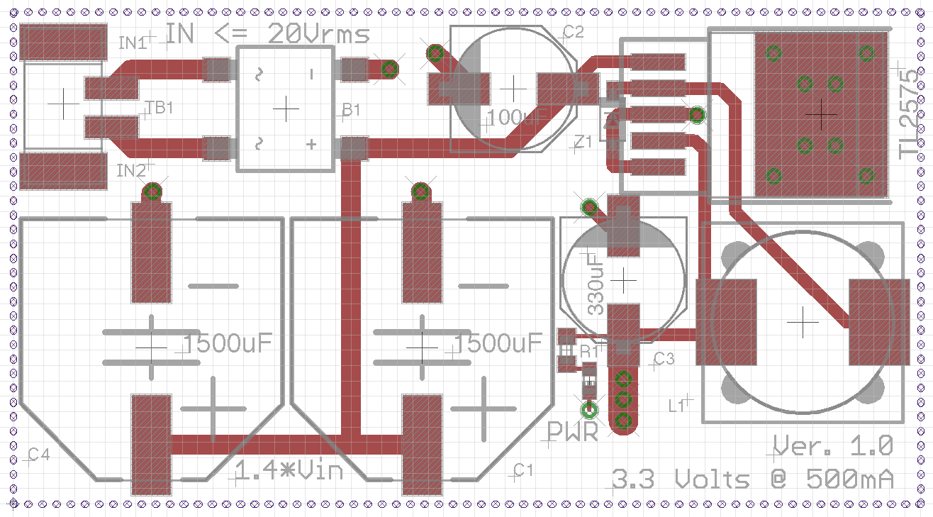
For myDoorbell I decided to use a 4-layer PCB process. This process has a layer of copper on the top and another on the bottom and two internal layers. The top and bottom layers are used to route interconnections. One of the internal layers is used to distribute 3.3 V to the entire system. The second internal layer is tied to ground and distributed throughout the design. These internal layers are often called planes. While myDoorbell is reasonably simple and might have been possible with a two layer design, having a ground and power plane results in a safe and simplified design. The top view of the resulting power supply PCB is shown below.

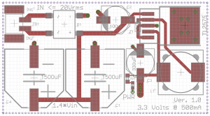
Those items represented in gray indicate labels and component outlines that will be visible on the completed board. The red areas represent the copper pads and interconnects on the top layer of the board. This board does not have any copper on the bottom layer. The green circles indicate where a via is used to connect the top copper to either the ground or 3.3 V planes. The dotted lines around the board represent the 3.3 V and ground planes.

In the upper left hand corner of the board there is a component we have not yet discussed. It is a simple connector where the two wires from the doorbell transformer are connected to the power supply. These feed directly into the full-wave bridge rectifier to the right. The positive output terminal of the rectifier is connected to the positive terminals of the capacitors, C1, C2, and C4, as well as the input of the regulator. The negative side of the rectifier is connected to ground through the via to its upper right. All other devices connected to ground do so through a via to the ground plane.

Due to the laws of physics, each wire is also an inductor and as such resit changes in current flow. The longer the wire, the more inductance it will have. For this reason it is good practice to minimize the length of wires connecting components, especially those that are high speed such as the switching regulator. You’ll notice that C1, C3, and Z1 are close to the regulator. One reason internal ground and power planes are useful is because they facilitate the close connection of components, reducing wire length, and inductance.

The large copper area in the upper right corner of the board connected to the ground plane through 8 via connections is where the regulator is physically connected to the board. The heat from the regulator flows through its body, onto this copper pad, and into the ground plane. This acts as a heatsink pulling the heat away from the device.

Note that the positive terminal of C3 connects to the 3.3 V internal plane through three via connections. Later this same 3.3 V plane will be connected to the rest of the myDoorbell circuit. The positive side of the rectifier component is the source of the 22.6 V that will be used by the audio amplifier.

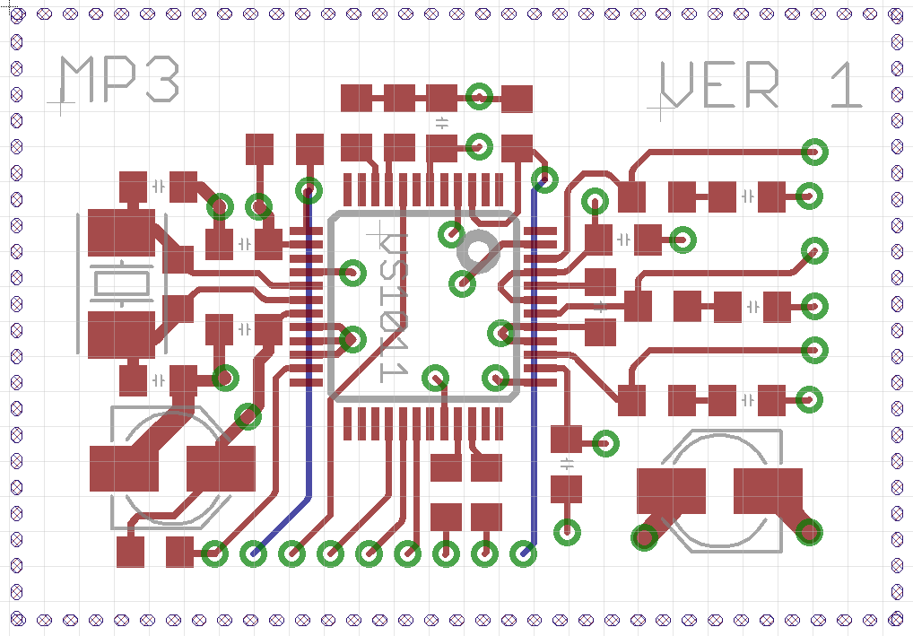
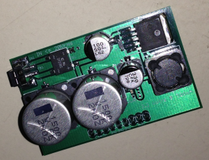
The resulting PCB measures 59mm in length and is 32mm wide. For testing purposes it was increased in size to allow for the inclusion of a set of header pins for easy insertion into a prototyping board. This breakout board is illustrated below. The tested board delivered 3.3 V at 400 mA and 22.6 V at nearly 1 A. This perfectly matches the needs of myDoorbell. Success at last!

Outcomes and Artifacts

Outcomes include lots of learning, a useful DC power supply design, and a working version implemented as a 4-layer PCB with surface mount components. The circuit is capable of inputs up to 20 Vrms resulting in a high voltage output of just over 28 V DC. By simply replacing the regulator with a product family substitute, the low voltage output can be changed to 5 V, 12 V, or 15 V. The schematic, PCB layout, and bill of materials can be acquired from github.

Basics to Remember

The relationship between peak and rms voltages is described by, Vrms = 0.707 * Vpeak.

Ohms Law states that voltage (V) is equal to the product of current (I) and resistance (R). voltage is measured in volts (V), current is measured in amperes (A) and resistance is measured in ohms (Ω).

Resistors (R) are measured in ohms (Ω), capacitors (C) are measured in farads (F), and inductors (L) are measured in henrys (H).

Due to the laws of physics, each wire is also an inductor and as such resit changes in current flow. The longer the wire, the more inductance it will have. For this reason it is good practice to minimize the length of wires connecting components, especially those that are high speed.

Component datasheets are our friends and we should get use to reading them, understanding them, and referring back to them often. They look long and complex, but you’ll get use to them.

Datasheets often have a “Typical Application” section that illustrates how the component can be used. This schematic can often be used as is or with minor modifications for your application.

LEDs can only handle so much current before their magic smoke escapes. The more current that flows through them, the brighter they are, within limits. 5 – 10 mA of current seems about right for many applications. The resistor in series with a LED is intended to limit the current. If you assume the voltage drop across a LED is 0 V, then the entire potential is across the resistor. Ohms Law states that the voltage is equal to the product of current and resistance, so the resistance is equal to the voltage divided by the current. In our example power supply, the voltage across the resistor is 3.3 V, so to limit the current to 5 mA we need a resistor of 3.3 V / 0.005 A = 660 Ω. Since resistors come in standard values we’ll use the closest standard value of 680 Ω.
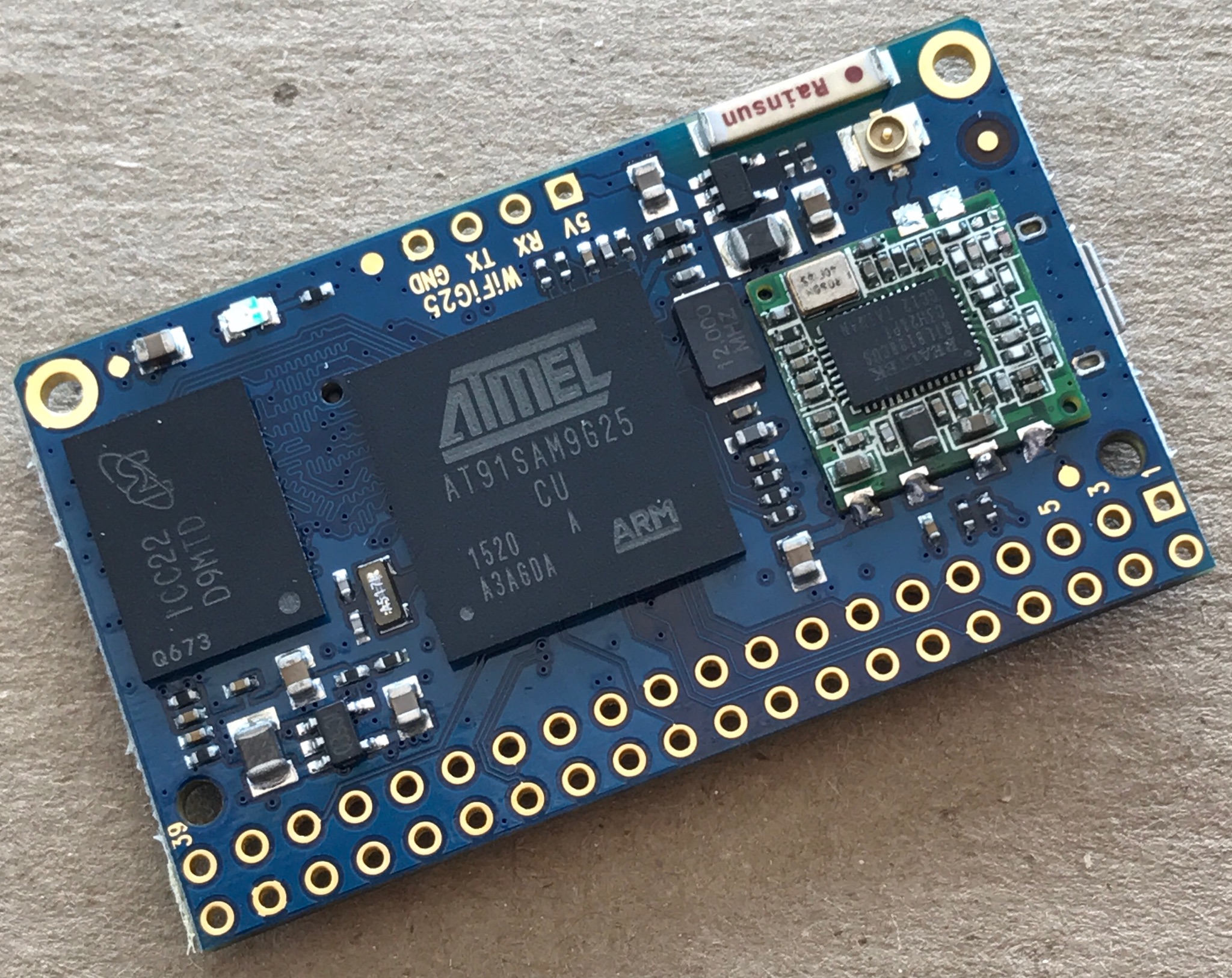
myDoorbell: High Level Design

Introduction

In my previous post I described the resources available in the wiring box where myDoorbell will be installed. As illustrated in the following figure, the available resources consist of a 16 Volt AC source and a connection to a doorbell button with an integrated lamp.

When the button is pressed, approximately 1 Ampere of current flows through the circuit. This current at 16 Volts AC yields 16 Watts of available power (16 Volts * 1 Ampere). This is sufficient for anything I am envisioning. For a more thorough, yet simple, explanation of Ohm’s Law click here.

Features and Hindsight

As pointed out in my first post on this subject, myDoorbell will have several unique characteristics or features:

  • Play ringtones uploaded by the user to celebrate seasons, holidays, birthdays, etc.
  • Record the time and date of each ring
  • Be configurable
  • Send a text message indicating a ring, if configured to do so
  • Be silent if configured not to make noise when babies are sleeping, pets shouldn’t be disturbed, or the owner just doesn’t want to know visitors are present
  • Access other Web resources such as APIs, webhooks, etc. 

As the saying goes, hindsight is 20/20. If I were designing myDoorbell all over again, I actually am, the next thing I would do is design the API that would describe the HTTP resources, methods, and error codes used to implement the above features and behaviors. However, when I began this adventure I didn’t know much about APIs, HTTP, and related technologies. Recall that this lack of knowledge was precisely why I started this adventure.

I will proceed in roughly the order I actually took, but want to encourage any readers creating hardware or software systems that they should design the API first. Since software is eating the world it is clear that any real system will contain software, and I believe that all such systems should have an API. Creating the API first will result in a better product and will reduce the risk of cresting hardware and software components that in the end are unnecessary.

Necessary Components 

Several hardware and software components are necessary to implement the characteristics and features listed above:

  • myDoorbell needs Internet connectivity to facilitate the uploading of ringtones, to enable the calling of other APIs or to raise events, and allow the acquisition of configuration information and updates. Since there is no wired network connection in the doorbell wiring box, this connectivity will be provided by a WiFi module. 
  • A microcontroller is needed to interact with the WiFi module, provide a compute platform for the web server implementing the myDoorbell API, interface with a nonvolatile memory, and enable the detection of the state of the doorbell button. 
  • A software module is needed that time slices between detecting the state of the doorbell button and dealing with incoming network traffic. It must also copy incoming ringtone data to the nonvolatile memory. Finally, this module must implement outgoing requests and the raising of events.
  • A simple hardware module is needed to provide doorbell button state information to the processor.
  • A nonvolatile memory is needed to store ringtones and configuration data. This memory needs to be writable by one microcontroller and readable by another, two ported.
  • A second microcontroller is needed to copy ringtone data from the nonvolatile memory to the audio system. 
  • An audio subsystem is necessary that converts mp3 encoded music to audio and amplifies the resulting audio to a sufficient amplitude to drive a speaker to the required volume.
  • A power supply is needed to convert the 16 Volt AC to a 3.3 – 5 Volt DC source for the digital electronics and a higher DC source for the audio amplifier. 

The following figure is a block diagram illustrating the hardware components listed above. Note that there are two modules for detecting the doorbell button state because most commercially available doorbells have the capability of ringing for both a front and rear door.

There are of course many ways to design any system, and I am not arguing that this is the best or even a reasonable design. In addition, as technology changes so do the choices and possible optimizations. My intent was to learn, and I learned a lot. In my next post I will describe the power supply module. This seems simple, but hang on and keep your arms and hands in the ride at all times!

myDoorbell: The Existing System

Introduction

In my previous post I declared my intent to refresh my technical skills through the development of an amazing doorbell, myDoorbell. In this post I describe a doorbell system found in a typical U.S. residence and discuss how this influenced the design of myDoorbell.

Typical Doorbell System

A typical doorbell system consists of several components: a doorbell button, a ringer mechanism / solenoid, and a doorbell transformer. These components are connected as illustrated in the following schematic.

When the doorbell button is pressed, AC flows through the solenoid causing it to strike a metallic bar tuned to create the expected “ding” sound. When the current is removed the solenoid is pulled back quickly by a spring, causing it to strike a second bar resulting in the anticipated “dong” sound. Many doorbell buttons have associated lamps to facilitate finding them in the dark. Like the button, the lamp also closes the circuit and energizes the solenoid. However, the resistance of the bulb limits the resulting current to a level that does not cause the solenoid to strike the metal chime.

In a sample system, acquired from a local home improvement store, the current through the solenoid was approximately 1 A when the button was pressed. When the button was not pressed the standby current was approximately 52 mA. A simple application of Ohm’s Law, 16V AC / 52mA, suggests that the resistance of the lamp is approximately 308 Ohms. When the lamp burns out, they always do, the standby current is reduced to zero.

One design decision I made early on was to enable myDoorbell to function with the existing doorbell button and transformer. In other words, myDoorbell would replace just the ringer portion of an existing system. In a common installation a pair  of wires from the button and a pair of wires from the transformer are brought to a wiring box where the ringer is installed. This is illustrated in the figure below.

The resources available in the wiring box are the connections to the push button, that requires 16V AC to power the lamp, and 16V AC. In my next post I’ll begin describing the design of myDoorbell based on the identified constraints and resources.

myDoorbell: A Learning Adventure

Introduction

After being a university chief information officer (CIO) for more than a decade, I decided to refresh my technical skills acquired through formal education and practice as an electrical engineer. I learn best by doing, so I picked a project I was interested in pursuing with the end goal being the learning, and not the finished product. I intend to share several posts that I hope illustrate the things learned and hope they are of value to the reader.

My Project

I have interest in the Internet of Things (IoT) movement and wanted to make strides towards making this practical, simple, and secure. I believe connected devices should be simple and consume little power. This likely requires devices that wake periodically, connect to some sort of network, and then go back to a low power state. After some experimentation it was clear, at the time, that WiFi was a real power hog and wasn’t a likely candidate. However, this realization led me to believe that another router, hub, or coordinator device would be necessary. I recall the effort required to convince homeowners to acquire WiFi routers and looked for an approach that would make this palatable.

I decided the answer was to create a product that homeowners would want to purchase because it excited them, and by the way it contained a network router / coordinator. Once acquired on its own merits, the product would facilitate the inexpensive and simple acquisition of other devices that connect to it. Products worth considering would be interesting to households and would connect to household power:

  • Lamps
  • Televisions or other audio / video (AV) equipment
  • Thermostats
  • Doorbells

Lamps seem simple and boring. However, after implementing my first choice, I know I should have chosen a lamp because it would have been boring, simple, and done! I decided embedding anything in televisions or other AV equipment would require skills and resources I didn’t have. Nest took the thermostat direction and while I disagree on the approach of putting so much technology in a tightly coupled system, I didn’t want everyone to judge my work against a commercially available product. I chose to implement a doorbell because they are ubiquitous, simple and meet my requirements:

  • They are in nearly every U.S. household.
  • Power is available where the indoor ringer is found.
  • They do one thing and no one cares if they do anything else.
  • They are in a good physical location for a network router.
  • They are out of the way, aren’t moved, never unplugged, or inadvertently reconfigured.

I chose to create a doorbell that would function as a replacement doorbell, would act as an IoT network router, and connect this network to the Internet by also connecting to an existing WiFi network. A quick trip to Home Depot revealed that an inexpensive doorbell cost about $13. Even with no experience in product development, I knew I wasn’t going to be able to build a doorbell that also acted as an IoT to WiFi gateway for $13. To be compelling enough to get households to acquire my doorbell it would have to be feature rich:

  • This doorbell would play ringtones uploaded by the user to celebrate seasons, holidays, birthdays, etc.
  • Each time someone rings this doorbell the time and date should be logged.
  • The owner can configure the bell to text them when someone rings.
  • The bell should be easily configured not to make noise when babies are sleeping, pets shouldn’t be disturbed, or the owner just doesn’t want to know you’re there.
  • When the bell is rung it should be configurable to access other Web resources such as APIs, webhooks, etc.
  • The system should be controlled and configured using a mobile app.
  • The doorbell must be a simple replacement of the original doorbell ringer.

While these features increase the likelihood of making it compelling enough to overcome the necessary price point, it certainly eliminates any chance of it being simple.

Summary

In this post I declared my intent to refresh my technical skills through the development of an IoT product, an amazing doorbell, myDoorbell. In the next few posts I will describe how a typical doorbell works, illustrate the general system layout for this new doorbell, describe how to create it so it fits into existing doorbell systems, and discuss many details of the techniques and technologies that make this possible. It will be a fun journey with many twists and turns, but that’s how learning happens!

Docker for Cross Compilation

Given my interests in enterprise computing and embedded systems, I decided to mix the two disciplines and use Docker to create a C development environment to generate Arm executable from my OS X based Mac. This may seem like a stretch, but the traditional way to do this is to fire up a full-blown virtual machine, install Linux, install the gcc based cross compiler, edit code on the host machine, switch to the VM, compile, and iterate.  This is slow and cumbersome, and not nearly as educational or fun!

The first step was to install boot2docker and follow the directions. This provided a simple and clean way to get Docker running on OS X.  Next I created a Dockerfile to create a Docker image FROM Ubuntu, loaded all the required modules and configured the image for cross compilation.  Here is my Dockerfile:

##################################################
# This docker file creates an Arm cross compiler
# platform from Ubunto
##################################################
# Ubunto as base image
FROM ubuntu
MAINTAINER J. Kelly Flanagan, Brigham Young University
# update ubuntu image
RUN apt-get update
# enable 32 bit code to run on 64 bit machine
RUN apt-get -y install lib32z1
# install the gcc tools to enable compilation
RUN apt-get -y install gcc build-essential libncurses5-dev mtd-utils u-boot-tools
# ADD cross compiler tools and unpack in appropriate location
# create destination directory
RUN mkdir /opt/codesourcery/
# ADD source
ADD arm* /opt/codesourcery/
ADD mkubifsimage /bin/
RUN chmod 777 /bin/mkubifsimage
# for interactive use set path
RUN echo ‘PATH=/opt/codesourcery/arm-2011.09/bin:$PATH’ >> /root/.bashrc
# set environment variable so I know I’m in a container
ENV ARM_CROSS_COMPILER TRUE
# create build directory where a volume will be mounted
RUN mkdir -p /tmp/arm_cross_compiler
# End Dockerfile

With this Dockerfile I ran the following build command using docker,

docker build -t ubuntu_arm_crosscompiler .

this resulted in a new Docker image called ubuntu_arm_crosscompiler. This image can be used to create an interactive Docker container by executing,

docker run -i -t ubuntu_arm_crosscompiler

This yields a shell where you can invoke gcc to create Arm object and executable files from source. However, I don’t use it interactively; I invoke it from make so that it appears as if I am compiling from my Mac, but end up with the desired Arm executable file.

As an example let’s assume we have a source directory with a Makefile and a few source files: Makefile, test.c, test.h, and testfunc.c.  The Makefile uses conditionals to determine whether it is executing on the host machine or the Docker container. In the Dockerfile the environment variable ARM_CROSS_COMPILER was set and will exist in any container derived from that image. The contents of the Makefile are included below.

# Name: Makefile
# Purpose: Build Arm executable via Docker based cross compiler
# Author: J. Kelly Flanagan
# Docker specific stuff
DOCKER_ARGS = -v $(PWD):/tmp/arm_cross_compiler -w /tmp/arm_cross_compiler
CC=/opt/codesourcery/arm-2011.09/bin/arm-none-linux-gnueabi-gcc
RM=rm -f
HEADERS = test.h
OBJECTS = test.o testfunc.o
TARGET = test
test: $(OBJECTS)
ifeq ($(ARM_CROSS_COMPILER),TRUE)
            $(CC) -o $@ $^ $(CFLAGS)
else
            @docker run $(DOCKER_ARGS) ubuntu_arm_crosscompiler make $@
endif
%.o: %.c $(HEADERS)
ifeq ($(ARM_CROSS_COMPILER),TRUE)

            $(CC) -c -o $@ $

else
            @docker run $(DOCKER_ARGS) ubuntu_arm_crosscompiler make $@
endif
clean:
            $(RM) $(OBJECTS) $(TARGET)

From the source directory we execute make and the first target (test) is invoked. This target invokes the next that checks to see if the header file or the source files are newer than the corresponding object files. If the object file doesn’t exist or the source file has been modified, the action is taken. The action checks to see if the ARM_CROSS_COMPILER environment variable is set. If it is not then the Docker command is executed. When the Docker container is created from the image it mounts the current working directory and executes the same make command that was invoked on the Mac. However, in the container the environment variable is set and the source file is compiled to an object file using the cross compiler. The make in the container now completes and returns to make on the Mac that then moves on to the next target. This is repeated until all object files have been created or updated at which point a final compilation takes place to link the object files to one executable.

Docker works well in this case because it is efficient enough to be invoked and destroyed quickly enough to not be a major contributor to compile time and it is much more convenient than switching back and forth between my host and a VM. Finally, I can share either the Dockerfile or the image with others, enabling them to easily use my tool chain. I’m definitely adding Docker to my standard set of tools for solving problems.

Criminals, Conjecture and Connected Things

My connected devices were initially secured using a hash-based message authentication code (HMAC).  An HMAC is constructed for each HTTP request directed at a device. The HMAC is created by combining some of the HTTP header elements, the time and date, the body of the request and a secret key / passwd.  The output block is then attached to the header of the request and transmitted to the selected device.  Upon reception of the request, the device collects the same header information, the time and date, and the body of the message and computes the HMAC using the same secret key / passwd.  If the computed HMAC and the one  sent with the request match, then the request is fulfilled.

While this protects the device from being compromised and the data being changed, it does nothing to protect the data from being read by prying eyes.  At first glance this seems unimportant since the data, inadvertently or intentionally, viewed by others carries little information.  For example, why would we care if others know the temperature of some sensor in our home? Why would it matter if someone knows the ringtone loaded in to our doorbell? Why would it matter if others know the setting on our thermostat?  Well each on their own might not matter, but with perhaps hundreds of devices in our home we offer up a lot of unprotected data for criminals to conjecture with.

Imagine a criminal mastermind sniffs your unprotected data and learns that your thermostat was just set to 55 degrees and the dog bark ringtone was loaded into your doorbell. In addition, late in the evening the temperature in the home is 55 degrees.  It wouldn’t be difficult to conjecture that no one is home.  In addition, the dog bark ringtone may lead them to believe that your gone for a while.

This simple example is intended to show that while we might erroneously think that this data does not need to be protected, it does!  In addition to protecting the device from intruders using HMAC, the data needs to be encrypted using SSL or other techniques.  By securing both, your connected devices and your data you will reduce the chance of having your virtual and physical spaces compromised by criminals.

css.php