Introduction
In a previous post, I described the nine modules that make up myDoorbell. These are shown in the following figure. In this post I’ll address two modules that are difficult to describe separately, the microcontroller near the center of the figure and the MP3 decoder to its right.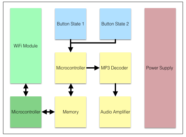
Basic Operation
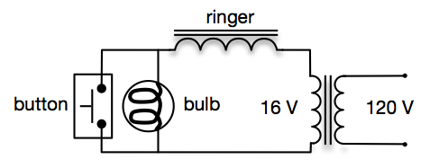
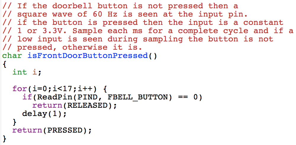
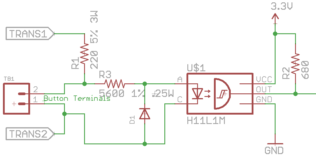
In my previous post I described a circuit that will translate a doorbell button press to a signal appropriate for consumption by the microcontroller. When this signal is received by the microcontroller, it takes two actions:
- It raises a signal to the second microcontroller enabling it to raise external events. These events will be discussed in a future post.
- It reads a MP3 encoded audio file from the memory and writes it to the MP3 Decoder module.
The MP3 Decoder module receives the streamed data from the microcontroller and decodes it, resulting in a small signal audio output.
The Microcontroller and Software
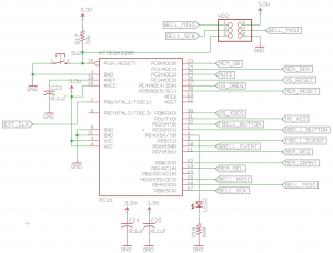
The microcontroller chosen for this application is the Atmel Atmega 328P. This processor is simple to use, relatively inexpensive and more than meets the requirements for this portion of myDoorbell. The schematic below illustrates the circuit used for this application. The labelled input and output signals are grouped into several main functions:
- Input from the doorbell button detection circuit described in the previous post.
- FBELL_BUTTON and RBELL_BUTTON
- Output signals to the second microcontroller.
- FBELL_EVENT and RBELL_EVENT
- Serial Peripheral Interface (SPI) signals for communicating to the MP3 decoder and programming this microcontroller
- BELL_SCK, BELL_MISO and BELL_MOSI
- Memory control and data signals
- MEM_SEL, MEM_GRANT, MEM_REQ, MEM_RESET, MEM_RDY and MEM_SB
- MP3 decoder control and data signals
- VS_XCS, VS_XDCS, VS_DREQ, VS_RESET and MUTE
- An external clock running at approximately 8 MHz.
- EXT_CLK
- EXT_CLK
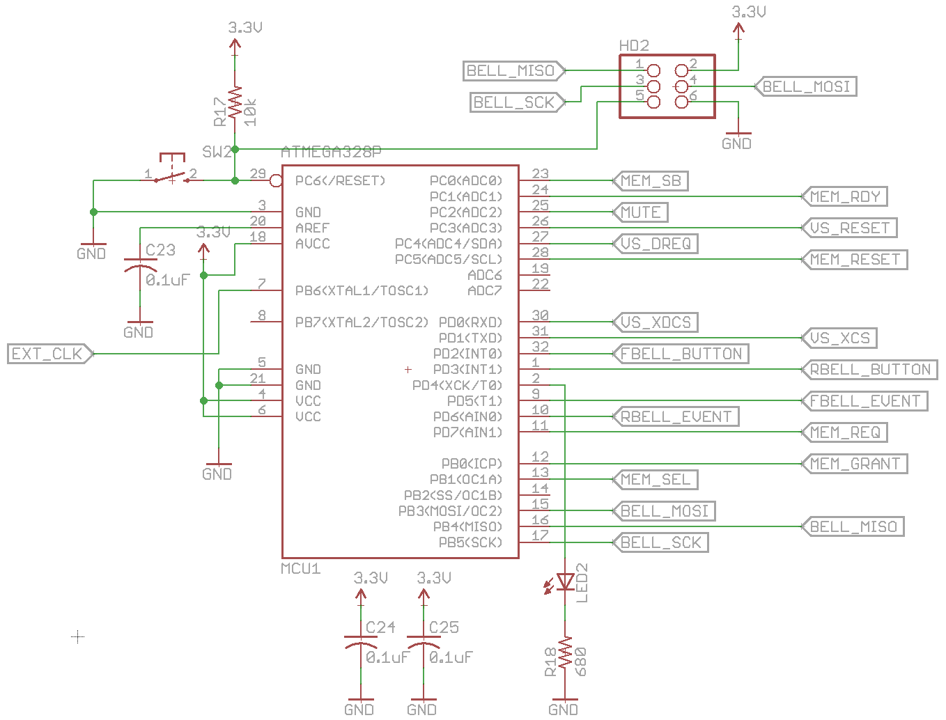
The LED and the associated current limiting resistor are available as a programmable output that is easily visible. This can be used to indicate state or for initial debugging. The push button enables the device to be manually reset. The capacitors are 0.1 µF devices that act as bypass capacitors, see Basics to Remember below. The six pin header, in the upper right corner of the schematic, is for programming the microcontroller.
The software that drives the signals identified above can be found in the myDoorbell repository on github.com. While there is considerable amount of detail, that is best addressed by viewing the source code, a brief overview is useful.
The “main” routine initializes the memory module and the MP3 Decoder module by communicating with them over the identified control and data lines. This communication takes place using the SPI protocol. This routine then loops checking the state of the front and rear doorbell buttons and requesting or relinquishing control of the memory device to / from the second microcontroller.
If the front or rear doorbell buttons are pressed, the microcontroller accesses its built in EEPROM to determine the volume at which the ringtone should be played. It then plays the appropriate ringtone for the front or rear door.
The ringtone is played by determining its length and repeatedly reading portions of it from the memory and streaming it to the MP3 decoder. When the data is consumed the device goes back to checking the state of the doorbell buttons.
The MP3 Decoder
The MP3 decoder is based on the VS1011 MP3 Audio Decoder. The following schematic is recreated from it datasheet.
The input and output signals, on the left of the schematic, are connected to the identically named signals from the microcontroller schematic already presented. The outputs on the right are the two audio output signals and the common between them. Lots of bypass capacitors and a few other components, as illustrated in the datasheet, are included.
The VS1011 is capable of consuming MP3 and WAV formatted audio files and generating low level audio output. The audio output is sufficient to drive a pair of headphones, but in our application will drive an audio amplifier and associated speaker.
A Failed First Attempt
The first design had a serious flaw that only manifested itself when in use. This misstep led to the design described in this post. However, since this design was put into use, two others have been proposed and will be described later.
The first design had a single microcontroller that interacted with the WiFi module, the doorbell button circuitry, the memory and the MP3 decoder. There was a major issue with this approach. When the doorbell button was pressed, should the MP3 file be played before an event is sent to the user, such as a text message, or should the event be raised and then the ringtone played?
If the event is sent first it will delay the playing of the ringtone by at least hundreds of milliseconds, but often much more. This doesn’t sound like much, but when you push a doorbell button you expect to hear the bell. In practice it was very odd to push the button and not get immediate feedback.
If you play the ringtone first and then send an event it works great, unless someone picks a 30 second ringtone. In this case, by the time you receive the text message and arrive at the door, the person is long gone. I have personally found that this behavior is often a feature, but others disagree.
This issue led to the design described here where we have two processors that communicate via shared signals and a shared memory. This approach is obviously more complex and more expensive.
Physical Implementation
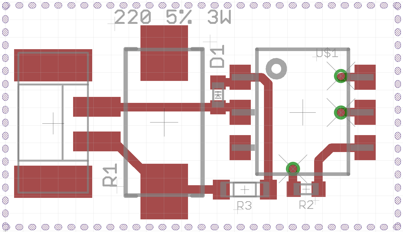
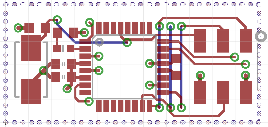
The schematic for the microcontroller shown above resulted in the following PCB layout.
This design required a few traces to be routed on the bottom layer. As with previous PCBs illustrated in this series of posts, this one also utilizes a 4-layer design with internal layers carrying ground and 3.3 V. The reset button is on the far left, the microcontroller in the center and its programming header on the right.
The schematic for the MP3 decoder, illustrated above, results in the following 4-layer PCB. The crystal that controls the clock for this unit is located on the left of the layout. Most of the input and output lines are located at the bottom of the board. The low level
audio output interface is located on the right. As in previous layouts, bypass capacitors and other components are placed as close to the device as possible. 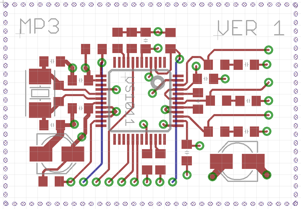
Two Alternative Designs
The first alternative design is based on the initial single CPU misstep. In the first design the problem was dealing with which came first, the raising of external events or the playing of the ringtone. A better approach may be to send the MP3 decoder the first 32 bytes of MP3 data and then start raising the external event. The MP3 decoder has a data request (DREQ) line that gets asserted whenever the decoder is capable of receiving another 32 bytes of MP3 data. If this were tied to the microcontrollers interrupt line it could be used to direct the microcontroller to send more audio data and then return to raising the event. The only question is whether the 8 MHz microcontroller is fast enough to switch between the two tasks and accomplish what needs to be done without introducing gaps in the ringtone.
Back of the envelope analysis to figure out if this would work goes something like this. Good quality stereo MP3 files are about 1 Mbyte per minute in size. Since we only need one channel we can reduce the file size to 500 Kbytes per minute. We can clock SPI data into the MP3 module at 4 MHz or 4 Mbits per second. With 8 bits per byte this translates to 500 Kbytes per second. With switching time between tasks and other overhead this won’t work, but it is likely that we can get by with far less quality than we expect from our digital stereo music. Reducing the quality will likely make this technique possible.
The second alternative design takes a radically different approach. For this approach we trade out the WiFi module, both microcontrollers, memory, and the MP3 decoder and replace it with a fast embedded ARM microcontroller that runs the Linux operating system. An example of this is the Onion, shown below.
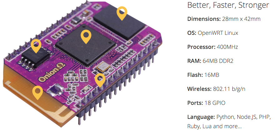 The microcontroller runs at 400 MHz instead of 8 MHz, giving us plenty of horsepower to accomplish our task. The Linux operating system provides the task switching necessary to switch rapidly between raising external events and playing ringtones. Audio playback software can be used instead of the dedicated MP3 decoder hardware currently being used. Finally, this sort of board costs less than $20, which is less than the WiFi module used in the current approach. This approach is currently being pursued.
In my own defense let me state that these sorts of modules were not available when the first design was completed. In addition, education leads to doing things in a better way; I’ve learned a lot!
Outcomes and Artifacts
There are likely many ways to build this portion of myDoorbell and a few of them have been described. The Eagle schematic and PCB files are available from the myDoorbell repository at github.com.
Basics to Remember
Bypass capacitors are used in many digital systems. Each clock cycle a digital system has the potential to change from one state to another. When this occurs the device draws significantly more current for a very short period of time. Recall that every wire acts like an inductor and that inductors resist changes in current. If the PCB trace from the device to the power source is long or narrow it will restrict current sufficiently to starve the device from the energy that it needs during these transition periods. Bypass capacitors hold sufficient charge to supply the device with the needed energy during these short periods of time. They are recharged while the device is relatively stable. These capacitors should be located as close to the device as possible and located between the power source and the device. This close proximity will reduce the inductance of the connecting trace.